- 您现在的位置:买卖IC网 > Sheet目录324 > FAN3217TMX (Fairchild Semiconductor)IC GATE DRIVER DUAL 2A 8-SOIC
�� �
�
�Applications� Information�
�Input� Thresholds�
�The� FAN3216� and� the� FAN3217� drivers� consist� of� two�
�identical� channels� that� may� be� used� independently� at�
�rated� current� or� connected� in� parallel� to� double� the�
�individual� current� capacity.�
�The� input� thresholds� meet� industry-standard� TTL-logic�
�thresholds� independent� of� the� V� DD� voltage,� and� there� is�
�a� hysteresis� voltage� of� approximately� 0.4� V.� These�
�levels� permit� the� inputs� to� be� driven� from� a� range� of�
�input� logic� signal� levels� for� which� a� voltage� over� 2� V� is�
�considered� logic� HIGH.� The� driving� signal� for� the� TTL�
�inputs� should� have� fast� rising� and� falling� edges� with� a�
�slew� rate� of� 6� V/μs� or� faster,� so� a� rise� time� from� 0� to�
�3.3� V� should� be� 550� ns� or� less.� With� reduced� slew� rate,�
�circuit� noise� could� cause� the� driver� input� voltage� to�
�exceed� the� hysteresis� voltage� and� retrigger� the� driver�
�input,� causing� erratic� operation.�
�Static� Supply� Current�
�In� the� I� DD� (static)� typical� performance� characteristics�
�shown� in� Figure� 10� and� Figure� 11,� each� curve� is�
�produced� with� both� inputs� floating� and� both� outputs�
�LOW� to� indicate� the� lowest� static� I� DD� current.� For� other�
�states,� additional� current� flows� through� the� 100k� Ω�
�resistors� on� the� inputs� and� outputs� shown� in� the� block�
�diagram� of� each� part� (see� Figure� 6� and� Figure� 7)� .� In�
�these� cases,� the� actual� static� I� DD� current� is� the� value�
�obtained� from� the� curves� plus� this� additional� current.�
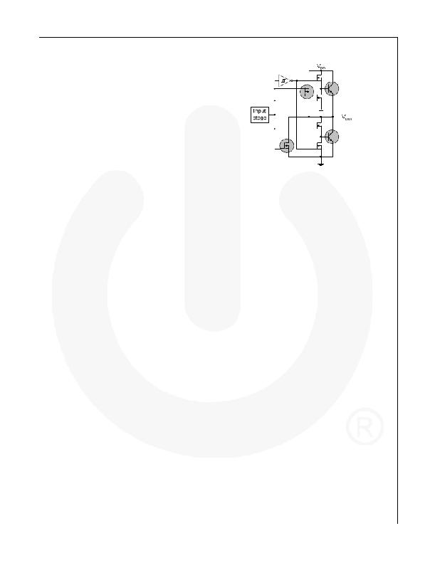
�MillerDrive?� Gate� Drive� Technology�
�FAN3216� and� FAN3217� gate� drivers� incorporate� the�
�MillerDrive?� architecture� shown� in� Figure� 31.� For� the�
�output� stage,� a� combination� of� bipolar� and� MOS� devices�
�provide� large� currents� over� a� wide� range� of� supply�
�voltage� and� temperature� variations.� The� bipolar� devices�
�carry� the� bulk� of� the� current� as� OUT� swings� between� 1/3�
�to� 2/3� V� DD� and� the� MOS� devices� pull� the� output� to� the�
�HIGH� or� LOW� rail.�
�The� purpose� of� the� MillerDrive?� architecture� is� to�
�speed� up� switching� by� providing� high� current� during� the�
�Miller� plateau� region� when� the� gate-drain� capacitance� of�
�the� MOSFET� is� being� charged� or� discharged� as� part� of�
�the� turn-on� /� turn-off� process.�
�For� applications� with� zero� voltage� switching� during� the�
�MOSFET� turn-on� or� turn-off� interval,� the� driver� supplies�
�high� peak� current� for� fast� switching� even� though� the�
�Miller� plateau� is� not� present.� This� situation� often� occurs�
�in� synchronous� rectifier� applications� because� the� body�
�diode� is� generally� conducting� before� the� MOSFET� is�
�switched� ON.�
�The� output� pin� slew� rate� is� determined� by� V� DD� voltage�
�and� the� load� on� the� output.� It� is� not� user� adjustable,� but�
�a� series� resistor� can� be� added� if� a� slower� rise� or� fall� time�
�at� the� MOSFET� gate� is� needed.�
�?� 2009� Fairchild� Semiconductor� Corporation�
�FAN3216� /� FAN3217� ?� Rev.� 1.0.3�
�12�
�Figure� 31.� MillerDrive?� Output� Architecture�
�Under-Voltage� Lockout�
�The� FAN321x� startup� logic� is� optimized� to� drive� ground-�
�referenced� N-channel� MOSFETs� with� an� under-voltage�
�lockout� (UVLO)� function� to� ensure� that� the� IC� starts� up�
�in� an� orderly� fashion.� When� V� DD� is� rising,� yet� below� the�
�3.9� V� operational� level,� this� circuit� holds� the� output�
�LOW,� regardless� of� the� status� of� the� input� pins.� After� the�
�part� is� active,� the� supply� voltage� must� drop� 0.2� V� before�
�the� part� shuts� down.� This� hysteresis� helps� prevent�
�chatter� when� low� V� DD� supply� voltages� have� noise� from�
�the� power� switching.� This� configuration� is� not� suitable�
�for� driving� high-side� P-channel� MOSFETs� because� the�
�low� output� voltage� of� the� driver� would� turn� the� P-channel�
�MOSFET� on� with� V� DD� below� 3.9� V.�
�V� DD� Bypass� Capacitor� Guidelines�
�To� enable� this� IC� to� turn� a� device� ON� quickly,� a� local�
�high-frequency� bypass� capacitor,� C� BYP� ,� with� low� ESR� and�
�ESL� should� be� connected� between� the� VDD� and� GND�
�pins� with� minimal� trace� length.� This� capacitor� is� in�
�addition� to� bulk� electrolytic� capacitance� of� 10� μF� to� 47� μF�
�commonly� found� on� driver� and� controller� bias� circuits.�
�A� typical� criterion� for� choosing� the� value� of� C� BYP� is� to�
�keep� the� ripple� voltage� on� the� V� DD� supply� to� ≤� 5%.� This�
�is� often� achieved� with� a� value� ≥� 20� times� the� equivalent�
�load� capacitance� C� EQV� ,� defined� here� as� Q� GATE� /V� DD� .�
�Ceramic� capacitors� of� 0.1� μF� to� 1� μF� or� larger� are�
�common� choices,� as� are� dielectrics,� such� as� X5R� and�
�X7R,� with� good� temperature� characteristics� and� high�
�pulse� current� capability.�
�If� circuit� noise� affects� normal� operation,� the� value� of�
�C� BYP� may� be� increased,� to� 50-100� times� the� C� EQV� ,� or�
�C� BYP� may� be� split� into� two� capacitors.� One� should� be� a�
�larger� value,� based� on� equivalent� load� capacitance,� and�
�the� other� a� smaller� value,� such� as� 1-10� nF� mounted�
�closest� to� the� VDD� and� GND� pins� to� carry� the� higher-�
�frequency� components� of� the� current� pulses.� The�
�bypass� capacitor� must� provide� the� pulsed� current� from�
�both� of� the� driver� channels� and,� if� the� drivers� are�
�switching� simultaneously,� the� combined� peak� current�
�sourced� from� the� C� BYP� would� be� twice� as� large� as� when�
�a� single� channel� is� switching.�
�www.fairchildsemi.com�
�发布紧急采购,3分钟左右您将得到回复。
相关PDF资料
FAN3223CMX
IC GATE DVR DUAL INV 4A 8-SOIC
FAN3226CMPX
IC GATE DVR DUAL 2A 8-MLP
FAN3227TMPX
IC GATE DVR DUAL 2A 8-MLP
FAN3268TMX
IC BRIDGE DVR P/N-CH 2A 8SOIC
FAN3278TMX
IC BRIDGE DVR P-N 2A 30V 8-SOIC
FAN5331SX
IC LED DRVR WHITE BCKLGT SOT23-5
FAN5333ASX
IC LED DRVR WHITE BCKLGT SOT23-5
FAN5340MPX
IC LED DVR SYNC CC 8-MLP
相关代理商/技术参数
FAN3217TMX_12
制造商:FAIRCHILD 制造商全称:Fairchild Semiconductor 功能描述:Dual-2A, High-Speed, Low-Side Gate Drivers
FAN3217TMX_F085
功能描述:功率驱动器IC Intgrtd Load Switch RoHS:否 制造商:Micrel 产品:MOSFET Gate Drivers 类型:Low Cost High or Low Side MOSFET Driver 上升时间: 下降时间: 电源电压-最大:30 V 电源电压-最小:2.75 V 电源电流: 最大功率耗散: 最大工作温度:+ 85 C 安装风格:SMD/SMT 封装 / 箱体:SOIC-8 封装:Tube
FAN3223
制造商:FAIRCHILD 制造商全称:Fairchild Semiconductor 功能描述:Dual 4A High-Speed, Low-Side Gate Drivers
FAN3223_10
制造商:FAIRCHILD 制造商全称:Fairchild Semiconductor 功能描述:Dual 4A High-Speed, Low-Side Gate Drivers
FAN3223_11
制造商:FAIRCHILD 制造商全称:Fairchild Semiconductor 功能描述:Dual 4A High-Speed, Low-Side Gate Drivers
FAN3223_12
制造商:FAIRCHILD 制造商全称:Fairchild Semiconductor 功能描述:Dual 4A High-Speed, Low-Side Gate Drivers
FAN3223C
制造商:FAIRCHILD 制造商全称:Fairchild Semiconductor 功能描述:30V PMOS-NMOS Bridge Driver
FAN3223CMPX
功能描述:功率驱动器IC Dual 4A High-Speed Low-Side Gate RoHS:否 制造商:Micrel 产品:MOSFET Gate Drivers 类型:Low Cost High or Low Side MOSFET Driver 上升时间: 下降时间: 电源电压-最大:30 V 电源电压-最小:2.75 V 电源电流: 最大功率耗散: 最大工作温度:+ 85 C 安装风格:SMD/SMT 封装 / 箱体:SOIC-8 封装:Tube